Memory and System Bus
This is a part of Writing a RISC-V Emulator in Rust. Our goal is running xv6, a small Unix-like OS, in your emulator eventually.
The source code used in this page is available at d0iasm/rvemu-for-book/02/.
The Goal of This Page
In this page, we will implement a memory (DRAM) and a system bus. The memory is used to store and load data. The system bus is a pathway to carry data between the CPU and the memory.
These components enable to execute load and store instructions which are the
part of base integer instruction set. There are 7 load instructions (lb, lh,
lw, ld, lbu, lhu, and lwu) and 4 store instructions (sb, sh, sw,
and sd).
Define Modules
Rust has a powerful module system that can split code into logical units. Each unit is called a module.
First, we divide main.rs implemented in the previous section. The code of the
CPU is splited to a new file cpu.rs.
To define a CPU module, we need to mod keyword at the beginning of the
main.rs file. The use keyword allows us to use public items defined in the
CPU module.
main.rs
#![allow(unused)]
fn main() {
// This declaration will look for a file named `cpu.rs` or `cpu/mod.rs` and
// will insert its contents inside a module named `cpu` under this scope.
mod cpu;

// Use all public structures, methods, and functions defined in the cpu module.
use crate::cpu::*;
}
cpu.rs
#![allow(unused)]
fn main() {
// `pub` keyword allows other modules use the `Cpu` structure and methods
// relating to it.
pub struct Cpu {
    ...
}

impl Cpu {
    ...
}
}
Memory (DRAM)
The memory we going to implement is a dynamic random-access memory which is called DRAM. It is used to store/load data while the program is running.
We represent it as a Dram struct. It contains a vector of bytes as a member.
The vector of bytes in the Dram instance is initialized with the data
containing executable binary when it's created by Dram::new().
dram.rs
#![allow(unused)]
fn main() {
pub const DRAM_SIZE: u64 = 1024 * 1024 * 128; // 128MiB

pub struct Dram {
    pub dram: Vec<u8>,
}

impl Dram {
    pub fn new(code: Vec<u8>) -> Dram {
        let mut dram = vec![0; DRAM_SIZE as usize];
        dram.splice(..code.len(), code.iter().cloned());

        Self { dram }
    }
}
}
Load and Store Methods
There are load and store public methods for the Dram struct. Arguments in
each method are an address and the number of bits. The number of bits can be
8, 16, 32, and 64 bits.
dram.rs
#![allow(unused)]
fn main() {
impl Dram {
    ...
    pub fn load(&self, addr: u64, size: u64) -> Result<u64, ()> {
        match size {
            8 => Ok(self.load8(addr)),
            16 => Ok(self.load16(addr)),
            32 => Ok(self.load32(addr)),
            64 => Ok(self.load64(addr)),
            _ => Err(()),
        }
    }

    pub fn store(&mut self, addr: u64, size: u64, value: u64) -> Result<(), ()> {
        match size {
            8 => Ok(self.store8(addr, value)),
            16 => Ok(self.store16(addr, value)),
            32 => Ok(self.store32(addr, value)),
            64 => Ok(self.store64(addr, value)),
            _ => Err(()),
        }
    }
    ...
}
}
load8, load16, load32, and load64 (store* as well) are private
methods to help us operate the DRAM with the specific size of bits. The DRAM
is a little-endian system as described in the previous section so we need to be
careful the order of bytes.
The following code is load32 and store32 methods. The byte of a smallest
memory address (index) is stored at the least signigicant byte at the largest
and the byte of a largest memory address (index + 3) is stored at the most
significant byte of a word.
dram.rs
#![allow(unused)]
fn main() {
impl Dram {
    ...

    fn load32(&self, addr: u64) -> u64 {
        let index = (addr - DRAM_BASE) as usize;
        return (self.dram[index] as u64)
            | ((self.dram[index + 1] as u64) << 8)
            | ((self.dram[index + 2] as u64) << 16)
            | ((self.dram[index + 3] as u64) << 24);
    }

    fn store32(&mut self, addr: u64, value: u64) {
        let index = (addr - DRAM_BASE) as usize;
        self.dram[index] = (value & 0xff) as u8;
        self.dram[index + 1] = ((value >> 8) & 0xff) as u8;
        self.dram[index + 2] = ((value >> 16) & 0xff) as u8;
        self.dram[index + 3] = ((value >> 24) & 0xff) as u8;
    }
    ...
}
}
Add Dram to Module
Let's add the Dram as a module. Once adding one line at main.rs, dram.rs
can be included to the build target by cargo build and we can use methods
defined at dram.rs.
main.rs
#![allow(unused)]
fn main() {
mod dram;
}
From now on, we will add a new file as a module implicitly when it is added.
System Bus
A system bus is a component to carry data between the CPU and peripheral devices such as a DRAM. In actual hardware, there are 3 types of a bus. The 3 buses together are called a system bus.
- Address bus: carries memory addresses.
- Data bus: carries the data.
- Control bus: carries control signals.
Our implementation doesn't care the differences between them and a system bus just connects the DRAM (and other peripheral devices) to the CPU and carries memory addresses and data stored in the memory and between them.
The Bus struct has a dram member and other peripheral devices we will add
later. The Cpu struct now has a bus member in it instead of a dram
member so that the CPU can access the DRAM via a system bus.
bus.rs
#![allow(unused)]
fn main() {
pub struct Bus {
    dram: Dram,
}
}
cpu.rs
#![allow(unused)]
fn main() {
pub struct Cpu {
    pub regs: [u64; 32],
    pub pc: u64,
    pub bus: Bus,
}
}
Memory-mapped I/O
Memory-mapped I/O (MMIO) is a method performing input and output between the
CPU and peripheral devices. MMIO uses the same address space as both DRAM and
peripheral devices. It means you can use same load and store instructions
for accessing peripheral devices. When you access at a memory address, it can
connect to either a DRAM or a specific peripheral device via the system bus.
The system bus is responsible for a memory map in our implementation. A memory map is a structure of data which indicates how memory is laid out for a DRAM and peripheral devices. This can be different depending on a hardware system.
For example, virt machine in QEMU has the following memory map. In the virt machine, DRAM starts at 0x80000000. We're going to implement the same memory map as the map of a virt machine although we only have a part of the peripheral devices the virt machine has.
static const struct MemmapEntry {
    hwaddr base;
    hwaddr size;
} virt_memmap[] = {
    [VIRT_DEBUG] =       {        0x0,         0x100 },
    [VIRT_MROM] =        {     0x1000,        0xf000 },
    [VIRT_TEST] =        {   0x100000,        0x1000 },
    [VIRT_RTC] =         {   0x101000,        0x1000 },
    [VIRT_CLINT] =       {  0x2000000,       0x10000 },
    [VIRT_PCIE_PIO] =    {  0x3000000,       0x10000 },
    [VIRT_PLIC] =        {  0xc000000, VIRT_PLIC_SIZE(VIRT_CPUS_MAX * 2) },
    [VIRT_UART0] =       { 0x10000000,         0x100 },
    [VIRT_VIRTIO] =      { 0x10001000,        0x1000 },
    [VIRT_FLASH] =       { 0x20000000,     0x4000000 },
    [VIRT_PCIE_ECAM] =   { 0x30000000,    0x10000000 },
    [VIRT_PCIE_MMIO] =   { 0x40000000,    0x40000000 },
    [VIRT_DRAM] =        { 0x80000000,           0x0 },
};
There are load and store public methods for the Bus struct. Arguments in
each method are an address and the number of bits. The number of bits can be
8, 16, 32, and 64.
If the addr is larger than 0x80000000 defined as DRAM_BASE, we can access to the DRAM.
dram.rs
#![allow(unused)]
fn main() {
/// The address which dram starts, same as QEMU virt machine.
pub const DRAM_BASE: u64 = 0x8000_0000;

impl Bus {
    ...

    pub fn load(&self, addr: u64, size: u64) -> Result<u64, ()> {
        if DRAM_BASE <= addr {
            return self.dram.load(addr, size);
        }
        Err(())
    }

    pub fn store(&mut self, addr: u64, size: u64, value: u64) -> Result<(), ()> {
        if DRAM_BASE <= addr {
            return self.dram.store(addr, size, value);
        }
        Err(())
    }
}
}
Update the CPU
We're going to implement load and store instructions which are the part of base
integer instruction set. There are 7 load instructions, lb, lh, lw,
lbu, and lhu defined at RV32I and lwu and ld defined at RV64I. There
are 4 store instructions, sb, sh, and sw defined at RV32I and sd
defined at RV64I.
Fetch-decode-execute Cycle
We update the fetch-decode-execute cycle introduced in the previous page. The
emulator continues to execute the cycle until fetch or execute methods fail.
main.rs
fn main() -> io::Result<()> {
    ...
    loop {
        // 1. Fetch.
        let inst = match cpu.fetch() {
            // Break the loop if an error occurs.
            Ok(inst) => inst,
            Err(_) => break,
        };

        // 2. Add 4 to the program counter.
        cpu.pc += 4;

        // 3. Decode.
        // 4. Execute.
        match cpu.execute(inst) {
            // Break the loop if an error occurs.
            Ok(_) => {}
            Err(_) => break,
        }

        // This is a workaround for avoiding an infinite loop.
        if cpu.pc == 0 {
            break;
        }
    }
    ...
}
Fetch Stage
The next executable binary can be fetched from DRAM via the system bus we just created. The size of bits is 32 since the the length of one instruction in RISC-V is always 4 bytes. (Note: The length of one instruction can be 2 bytes in the compressed instruction set.)
cpu.rs
#![allow(unused)]
fn main() {
impl Cpu {
    ...
    pub fn fetch(&mut self) -> Result<u64, ()> {
        match self.bus.load(self.pc, 32) {
            Ok(inst) => Ok(inst),
            Err(_e) => Err(()),
        }
    }
    ...
}
}
Decode Stage
Load instructions are I-type and store instrucrtions are S-type format as we can
see them in Fig 2.1. and 2.2. The positions for rs1, funct3 (the 3 bits
between rs1 and rd), and opcode are the same position in the both format.
In RISC-V, there are many common positions in all formats, but decoding an immediate value is quite different depending on instructions, so we'll decode an immediate value in each operation.
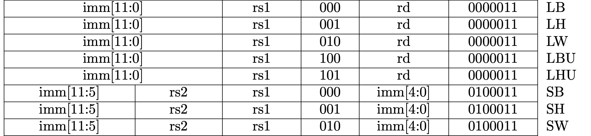
Fig 2.1 Load and store instructions in RV32I.

Fig 2.2 Load and store instructions in RV64I.
cpu.rs
#![allow(unused)]
fn main() {
impl Cpu {
    ...
    fn execute(&mut self, inst: u32) {
        ...
        let funct3 = ((inst >> 12) & 0x7);
        ...
        match opcode {
            0x03 => { // Load instructions.
                // imm[11:0] = inst[31:20]
                let imm = ((inst as i32 as i64) >> 20) as u64;
                let addr = self.regs[rs1].wrapping_add(imm);
                ...
            0x23 => { // Store instructions.
                // imm[11:5|4:0] = inst[31:25|11:7]
                let imm = (((inst & 0xfe000000) as i32 as i64 >> 20) as u64) | ((inst >> 7) & 0x1f);
                let addr = self.regs[rs1].wrapping_add(imm);
                ...
}
Decoding is performed by bitwise ANDs and bit shifts. The point to be noted is that an immediate value should be sign-extended. It means we need to fill in the upper bits with 1 when the significant bit is 1. In this implementation, filling in bits with 1 is performed by casting from a signed integer to an unsigned integer.
Execute Stage
Each operation is performed in each match arm. For example, a load
instruction lb is executed when opcode is 0x3 and funct3 is 0x0. The
lb instruction loads a byte from a DRAM with the specific addr position.
The suffix in load and store instructions mean the size of bits.
- b: a byte (8 bits)
- h: a half word (16 bits)
- w: a word (32 bits)
- d: a double word (64 bits)
Also, u in load instructions means "unsigned".
cpu.rs
#![allow(unused)]
fn main() {
impl Cpu {
    ...
    fn execute(&mut self, inst: u32) {
        ...
        match opcode {
            0x03 => { // Load instructions.
                // imm[11:0] = inst[31:20]
                let imm = ((inst as i32 as i64) >> 20) as u64;
                let addr = self.regs[rs1].wrapping_add(imm);
                match funct3 {
                    0x0 => {
                        // lb
                        let val = self.load(addr, 8)?;
                        self.regs[rd] = val as i8 as i64 as u64;
                    }
                    0x1 => {
                        // lh
                        let val = self.load(addr, 16)?;
                        self.regs[rd] = val as i16 as i64 as u64;
                    }
                    0x2 => {
                        // lw
                        let val = self.load(addr, 32)?;
                        self.regs[rd] = val as i32 as i64 as u64;
                    }
                    0x3 => {
                        // ld
                        let val = self.load(addr, 64)?;
                        self.regs[rd] = val;
                    }
                    0x4 => {
                        // lbu
                        let val = self.load(addr, 8)?;
                        self.regs[rd] = val;
                    }
                    0x5 => {
                        // lhu
                        let val = self.load(addr, 16)?;
                        self.regs[rd] = val;
                    }
                    0x6 => {
                        // lwu
                        let val = self.load(addr, 32)?;
                        self.regs[rd] = val;
                    }
                    _ => {}
                }
            }
            0x23 => { // Store instructions.
                // imm[11:5|4:0] = inst[31:25|11:7]
                let imm = (((inst & 0xfe000000) as i32 as i64 >> 20) as u64) | ((inst >> 7) & 0x1f);
                let addr = self.regs[rs1].wrapping_add(imm);
                match funct3 {
                    0x0 => self.store(addr, 8, self.regs[rs2])?,  // sb
                    0x1 => self.store(addr, 16, self.regs[rs2])?, // sh
                    0x2 => self.store(addr, 32, self.regs[rs2])?, // sw
                    0x3 => self.store(addr, 64, self.regs[rs2])?, // sd
                    _ => {}
                }
            }
            ...
}
Instruction Set
We've already implemented add and addi in the previous page and load and
store instructions in this page. These instructions are a part of base integer
instruction set (RV64I). To run xv6 in our emulator, we need to implement all
instructions in RV64I and a part of instructions in RV64A and RV64M.
Here is the page for all instruction set we need to implement for running xv6: